

1 day ago
India Notifies Rs 1.27 Lakh Crore Semicon 2.0 Programme
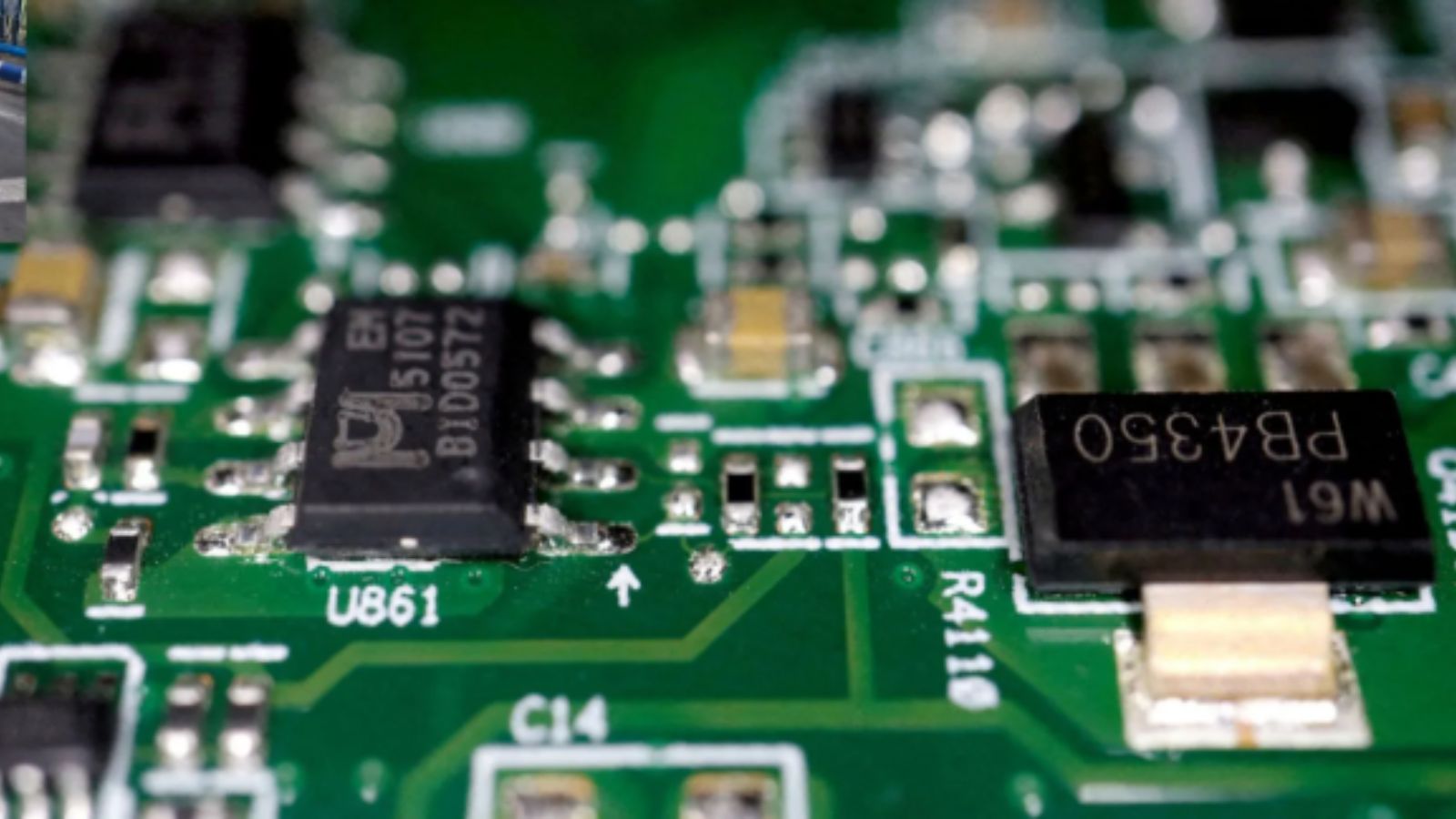
India has announced a large programme to help build more computer chips inside the country.
The programme is called Semicon 2.0 and is worth Rs 1.27 lakh crore.
It will help companies design chips, build factories and make equipment and materials.
Indian companies can get special help to create chips for important services and for commercial products.
Start-ups and small businesses can receive funding for their chip projects.
Large chip factories can receive support covering part of their construction costs.
The government will also support advanced ways of putting chips into packages.
It hopes the plan will create jobs, train engineers and make India less dependent on overseas suppliers.
The programme comes as demand for chips is increasing because of artificial intelligence and other technologies.

The government notified the Rs 1,27,500-crore Semicon 2.0 programme covering six pillars and 10 categories across the semiconductor value chain.
The scheme prioritises domestic chip design, offering support for strategic chips, commercial fabless companies and deployment of Indian-designed chips.
Large silicon wafer fabs can receive 40% capital-expenditure support, while compound semiconductor, display and advanced packaging projects can receive up to 35%.
Start-ups and MSMEs designing commercial chips can receive seed funding of up to Rs 15 crore or 50% of project costs, whichever is lower.
The programme also supports semiconductor equipment, materials, research, talent development and advanced packaging to reduce supply-chain dependence.
- Who
- The Government of India, through the Ministry of Electronics and Information Technology, will implement the programme for eligible semiconductor companies, start-ups, MSMEs and research organisations.
- What
- A Rs 1.27 lakh crore Semicon 2.0 programme has been notified, offering incentives across chip design, fabrication, packaging, equipment, materials, research and talent development.
- Where
- The programme will support semiconductor projects established in India, including Indian-headquartered chip-design companies and domestic manufacturing facilities.
- When
- The operational framework was notified on Monday, after the Union Cabinet approved the programme on July 15, 2026.
- Why
- The initiative aims to build a self-reliant semiconductor ecosystem, address supply-chain vulnerabilities and respond to rising global chip demand driven partly by artificial intelligence.
Key facts
- Total outlay
- Rs 1,27,500 crore
- Programme structure
- Six pillars and 10 categories
- Silicon fab support
- 40% of eligible capital expenditure
- Silicon fab threshold
- Minimum investment of Rs 20,000 crore and capacity of 40,000 300-mm wafer starts per month
- Commercial chip-design funding
- Start-ups and MSMEs can receive up to Rs 15 crore or 50% of project cost, whichever is lower
- Advanced packaging support
- 35% of eligible capital expenditure, compared with 25% for legacy packaging
- Research and talent support
- Up to 75% of project cost, including state incentives
Quotes

Ashwini Vaishnaw
India's IT Minister
“India achieved its target of developing 85,000 semiconductor engineers over a period of 10 years in just four years, and has now set a new target of developing one lakh more engineers… Students from tier-II and tier-III cities have already designed more than 250 chips… The semiconductor ecosystem being developed in India is also expected to create 50,000-60,000 direct jobs”
 indianexpress.com
“I was also glad to see that the scheme has this time been opened up to OCI companies owned by Overseas Citizens of India, which is a very good decision, since they bring rich global experience that will help create truly advanced design companies in India”
indianexpress.com
Sources
Related news

India Notifies ₹1.27 Lakh-Crore Semicon 2.0 Semiconductor Expansion Scheme
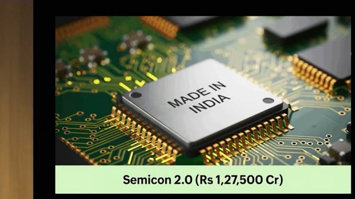
Govt Launches ₹1.27 Lakh Crore Semicon 2.0 Scheme

India Expands Semicon 2.0 With 100,000 Engineer Target
India’s Semicon 2.0 Broadens Chip Ecosystem; Three Stocks Watched
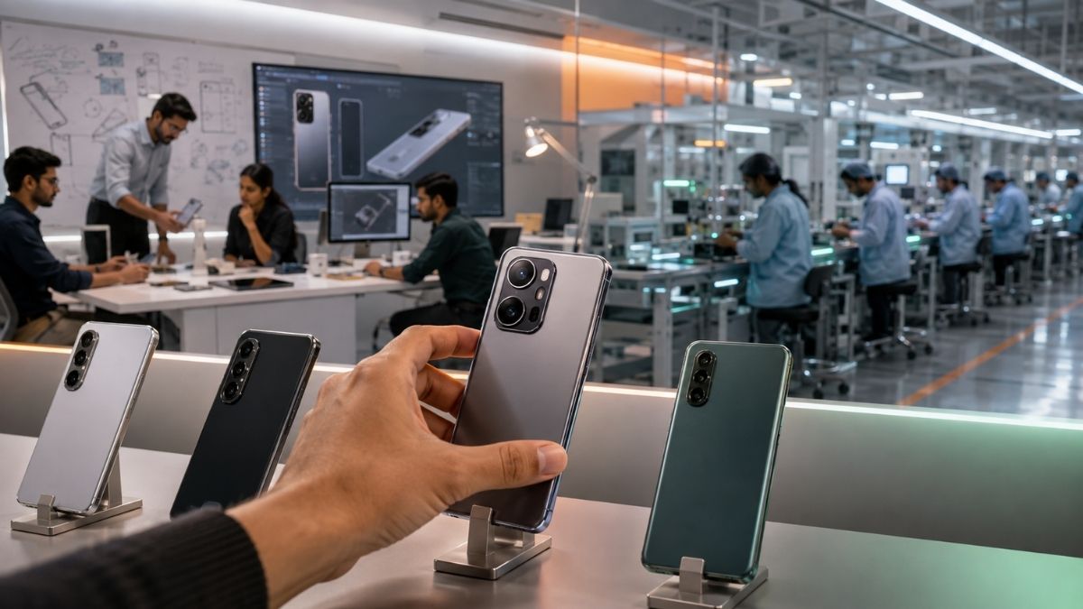
India's New Smartphone Scheme Faces Consumer Product Test
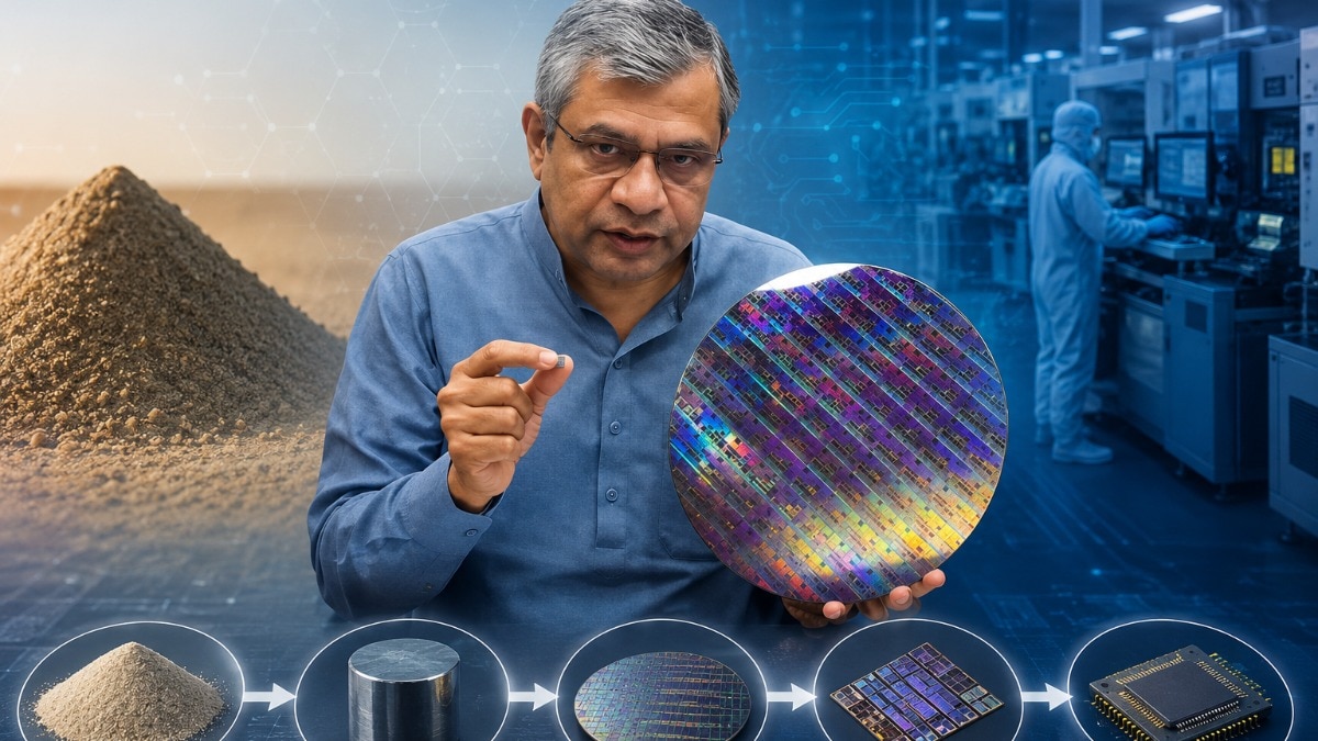
Vaishnaw Explains India’s Journey From Sand to Semiconductor Chips

Proposed Bullet Train Could Cut Delhi-Patna Travel Time

Adityanath Accuses Previous Governments of Hiding Encephalitis Deaths
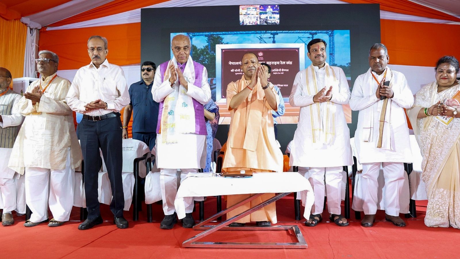
Upgraded Nepalganj Road-Bahraich Rail Section Inaugurated in Uttar Pradesh