

1 day ago
Vaishnaw Explains India’s Journey From Sand to Semiconductor Chips
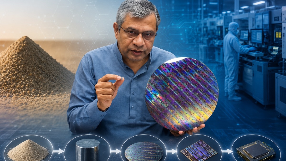
Computer chips start with silica-rich sand that is turned into a solid silicon cylinder called an ingot.
The ingot is sliced into very thin discs called wafers.
Tiny circuit patterns are then placed on the wafers with extraordinary precision.
Many layers are built, like floors in a very small building.
The wafer is cut into individual chips.
Each chip is assembled, tested, marked, and packaged before it can be used.
India is working to make more parts of this process inside the country.
The government says it wants to develop factories, suppliers, designers, and student talent for the long term.

Semiconductor production begins with silica-rich sand, which is made into silicon ingots and sliced into bare wafers.
Manufacturers etch extremely precise circuitry onto wafers through roughly 40 to 50 layers.
Individual chips are extracted from fabricated wafers and processed through assembly, testing, marking, and packaging.
India has approved 12 semiconductor plants under Semiconductor Mission 1.0, with three already manufacturing.
Ashwini Vaishnaw said Semicon 2.0 will build on this progress by developing India’s broader semiconductor ecosystem and design capabilities.
- Who
- IT Minister Ashwini Vaishnaw and the Indian government are leading the semiconductor initiative.
- What
- Vaishnaw explained how chips are made and described India’s efforts to build a complete semiconductor ecosystem.
- Where
- The initiative is focused on developing semiconductor manufacturing and design in India.
- When
- The article does not specify when Vaishnaw made the explanation.
- Why
- The government wants to establish a domestic semiconductor industry and develop the full value chain rather than only fabrication plants.
Key facts
- Starting material
- Silica-rich sand
- Manufacturing sequence
- Sand, silicon ingot, bare wafer, fabricated wafer, chip, and modules
- Wafer circuitry
- Approximately 40 to 50 layers
- Chip packaging process
- Assembly, testing, marking, and packaging, known as ATMP
- Approved plants
- 12 plants approved under Semiconductor Mission 1.0
- Plants manufacturing
- Three approved plants have started manufacturing
- Next phase
- Semicon 2.0
- Design ecosystem
- India’s semiconductor design ecosystem is described as very nascent
Quotes

Ashwini Vaishnaw
India’s IT minister and leader of the country’s semiconductor mission
“That is the level of precision which is required to be done while fabricating the chips.”
 businesstoday.in
“We didn't say just set up a fab. No. We need to develop the entire ecosystem.”
businesstoday.in
Sources
Related news
India Builds Semiconductor Ecosystem From Chips to Fabs

India's semiconductor push could define its AI ambitions
India's VIHAAN chip hits first-pass silicon success, eyes 2027 production

India’s Semiconductor Push Advances With Tata’s Dholera Fab

Aheesa’s VIHAAN-I advances India’s indigenous semiconductor design ambitions
India's New Smartphone Scheme Faces Consumer Product Test

Proposed Bullet Train Could Cut Delhi-Patna Travel Time

Adityanath Accuses Previous Governments of Hiding Encephalitis Deaths

Upgraded Nepalganj Road-Bahraich Rail Section Inaugurated in Uttar Pradesh