

1 day ago
Can Advanced Packaging Help India Enter the Global Semiconductor Race?
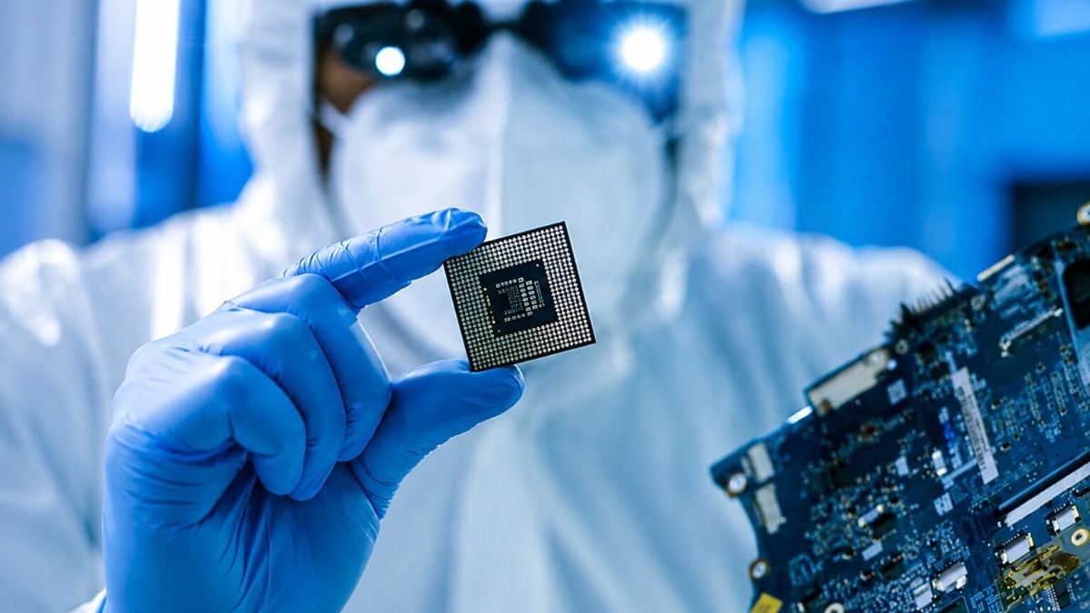
Making computer chips is becoming harder because shrinking their tiny parts costs more money.
Advanced packaging offers another way to make faster chips.
It puts several smaller chips, called chiplets, together inside one package.
This is especially useful for artificial intelligence systems that need very fast connections.
Building a packaging factory is generally cheaper and faster than building a cutting-edge chip factory, but it still requires billions of dollars.
India is offering financial support to attract these projects.
India also has engineering talent, lower costs and a large electronics market.
However, it needs more suppliers, equipment, materials and experienced workers.
Advanced packaging could help India enter the semiconductor industry faster, but it will not replace the need to develop broader chipmaking capabilities.

Advanced packaging combines chiplets or components to improve performance, power efficiency and manufacturing flexibility.
AI processors, data centers, automotive systems and high-performance computing are increasing demand for advanced packaging.
Advanced packaging facilities can cost $2 billion to $8 billion and take nearly three years to qualify for production.
India’s Semicon 2.0 offers advanced-packaging projects support of up to 35% of capital expenditure.
India has engineering talent and lower costs but lacks a mature local base of substrates, materials, equipment and packaging specialists.
- Who
- India, global chipmakers and packaging companies including TSMC, Intel, Samsung, Micron, ASE Group and Amkor Technology.
- What
- India is considering advanced semiconductor packaging as a faster entry point into the global chip industry.
- Where
- India, alongside packaging investments in locations such as Arizona and Malaysia.
- When
- The opportunity is emerging as advanced packaging demand grows, with the global market projected to expand from 2024 to 2030.
- Why
- Advanced packaging can improve chip performance and provide a lower-cost entry than building a semiconductor fabrication plant, while AI and other applications drive demand.
Advanced Packaging as an Opportunity
Advanced Packaging’s Limitations
Faster route into semiconductors
Advanced Packaging as an Opportunity
Packaging facilities generally require less capital and can reach production sooner than large semiconductor fabs, giving India a quicker path to commercial relevance.
Advanced Packaging’s Limitations
Lower entry costs do not eliminate capital intensity; advanced facilities can still cost up to $8 billion and require lengthy qualification and customer approval.
India’s competitive advantages
Advanced Packaging as an Opportunity
India offers engineering talent, lower costs, government incentives, a large electronics market and supply-chain diversification potential.
Advanced Packaging’s Limitations
India lacks a sufficiently developed local ecosystem of advanced substrates, materials, equipment and experienced packaging engineers.
Timing of the opportunity
Advanced Packaging as an Opportunity
India’s late start in conventional manufacturing may not be a disadvantage because chiplets and new integration technologies are creating new entry points.
Advanced Packaging’s Limitations
The opportunity is narrowing as companies build packaging capacity closer to their manufacturing sites and customers, making rapid development of infrastructure, talent and customers essential.
Key facts
- Global market size
- The advanced packaging market was valued at $20.2 billion in 2024 and is projected to reach $39.6 billion by 2030.
- Advanced packaging cost
- A commercially viable facility can require $2 billion to $8 billion.
- Production timeline
- Setup and qualification can take close to three years before high-volume manufacturing begins.
- Semicon 2.0 outlay
- India’s programme has an outlay of Rs 1.275 lakh crore.
- Advanced packaging incentive
- Eligible projects can receive support of up to 35% of capital expenditure.
- Fab comparison
- A mature-node fab can require $3 billion to $5 billion, while a leading-edge fab can cost more than $10 billion to $20 billion.
- India’s ecosystem gap
- The country has limited local capacity for advanced substrates, materials, equipment and experienced packaging engineers.
Quotes
Sanchit Vir Gogia
Chief analyst and CEO at Greyhound Research
“For years, chipmakers made chips faster by shrinking transistors. Now making transistors smaller is becoming harder and more expensive, so chipmakers are combining different chips, or chiplets, in one advanced package.”
 businesstoday.in
“Companies look for skilled talent, reliable power and water, good logistics, semiconductor suppliers, customers, government incentives and the ability to achieve high manufacturing yields.”
businesstoday.in
Sources
Related news
India Builds Semiconductor Ecosystem From Chips to Fabs

India's semiconductor push could define its AI ambitions

India builds domestic semiconductor and AI capabilities with major investments

Semicon India 2.0 Aims to Build Global Chip IP

Five High-Capacity Washing Machines for Families of Five

India’s Refurbished Smartphone Market Grows as New Prices Rise

Samsung Galaxy Watch 9 review praises comfort, performance, health tracking

Dolby Atmos Soundbars Compared: Immersion, Bass, Dialogue and Setup
