

2 hrs ago
India’s semiconductor strategy must move beyond chip packaging
Rajeev Chandrasekhar says India has made progress in building semiconductor factories.
However, he says many of the approved facilities mainly package and test chips.
Packaging is useful, but he believes it usually earns less than designing or manufacturing advanced chips.
He says artificial intelligence is changing what kinds of chips the world needs.
India may have an opportunity to build chips that run trained AI systems, called inference chips.
Chandrasekhar says India has 1.25 lakh chip-design engineers who could help with this work.
He also wants India to invest more in research, chip designs and advanced manufacturing.
His proposals include a research institute and a ₹1,000-crore fund.
He believes success should be measured by technological capability, not only by the number of factories approved.

Rajeev Chandrasekhar said India has approved 12 semiconductor manufacturing units with ₹1.64 lakh crore in committed investment.
He said five facilities are already in production and India Semiconductor Mission 2.0 involved another ₹1.275 lakh crore.
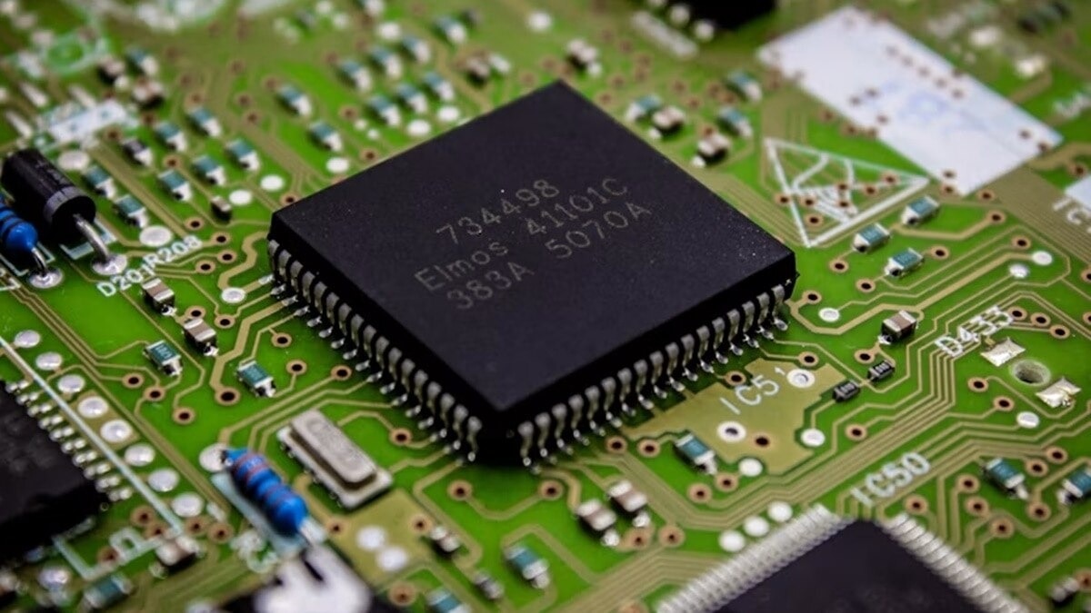
Chandrasekhar noted that nine of the 12 approved units are conventional ATMP/OSAT packaging and testing facilities.
He argued that India should prioritize chip design, intellectual property, advanced packaging and fabrication as AI reshapes the industry.
His proposals include a National Semiconductor Research Institute, a ₹1,000-crore chip design fund and government-backed inference-chip programmes.
- Who
- Rajeev Chandrasekhar, discussing India’s semiconductor strategy.
- What
- He called for India to move beyond conventional chip packaging toward design, intellectual property, advanced packaging, fabrication and AI inference chips.
- Where
- India and its semiconductor industry.
- When
- The article’s publication date is not specified; it cites a post dated October 2, 2026.
- Why
- Chandrasekhar argues that AI is reshaping the semiconductor industry and that India should capture more value through technological capability.
Key facts
- Approved units
- 12 semiconductor manufacturing units
- Committed investment
- ₹1.64 lakh crore
- Facilities in production
- Five
- India Semiconductor Mission 2.0
- Another ₹1.275 lakh crore in investment, according to Chandrasekhar
- Conventional facilities
- Nine of the 12 approved units are conventional ATMP/OSAT facilities
- Chip-design workforce
- 1.25 lakh chip-design engineers
- Proposed fund
- ₹1,000 crore Chip Design Commercialisation Fund
Quotes

Rajeev Chandrasekhar
Former Indian minister and semiconductor policy advocate
“Nine of those 12 approved units are conventional ATMP/OSAT facilities — wire-bond assembly, testing, marking, and packaging”
 businesstoday.in
“Semiconductors are not experiencing supply-chain diversification. They are experiencing an architectural revolution”
businesstoday.in
Sources
Related news
India’s Semicon 2.0 Expands Chip Ecosystem With $12 Billion
India’s Semiconductor Push Targets Global Product Champions Through R&D
India Expands Semiconductor Mission to Build Chips and Talent
India's Semiconductor Push Reaches Export Markets Amid Expansion Plans
India Expands Global Semiconductor Goals With Semicon 2.0
Modi Pitches India as Trusted Hub for Chip Manufacturing
Aheesa’s VIHAAN-I advances India’s indigenous semiconductor design ambitions

Karnataka Launches KEO AI Computers for Government Schools

IIT Madras to host symposium on semiconductor future