
1 week ago
How a Pen Accident Helped Create Modern Computer Chips
In 1916, a scientist accidentally dipped a pen into melted tin.
When he pulled it out, a thin strand of metal formed.
He studied this surprising result instead of ignoring it.
He discovered that carefully pulling material from a hot liquid could grow one large, orderly crystal.
This became known as the Czochralski method.
Many years later, scientists used the method to grow crystals of silicon.
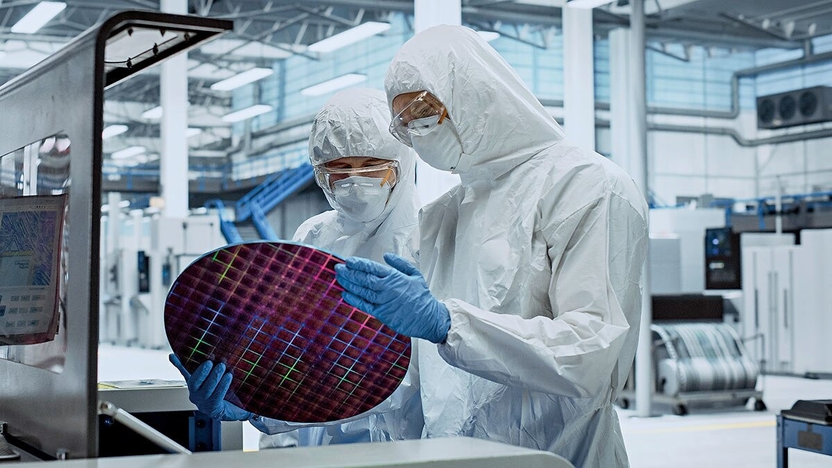
Large silicon crystals are sliced into thin discs called wafers.
Electronic circuits are made on these wafers.
Those circuits are the tiny parts found inside computer chips.

In 1916, a pen dipped into molten tin accidentally produced a thin metallic filament.
Jan Czochralski investigated the filament and developed a method for pulling crystals from molten material.
The Czochralski method controls pulling speed, rotation and temperature to grow single crystals.
Decades later, the technique was adapted to germanium and then silicon for semiconductor manufacturing.
Large silicon crystals are sliced into wafers on which microscopic electronic circuits are built.
- Who
- Czochralski and later semiconductor scientists used the crystal-growing technique.
- What
- An accidental pen experiment led to the Czochralski method for growing single crystals used in silicon wafer production.
- Where
- The accident occurred in a laboratory, but the article does not specify its location.
- When
- The original work was submitted in 1916 and published in 1918; its semiconductor applications emerged decades later.
- Why
- The method provided large, uniform single-crystal semiconductor materials needed to manufacture electronic circuits.
Key facts
- Accident
- A pen dipped into molten tin produced a strange metallic filament.
- Original research
- Czochralski was studying the crystallisation rate of metals.
- First publication
- The method was described in a paper submitted in 1916 and published in 1918.
- Method
- A small crystal seed is touched to molten material and slowly pulled upward.
- Materials
- The technique was adapted first to germanium and subsequently to silicon.
- Wafer production
- Large cylindrical silicon ingots are sliced into thin wafers.
- Manufacturing role
- Electronic circuits are manufactured on the surface of silicon wafers.
Sources
Related news
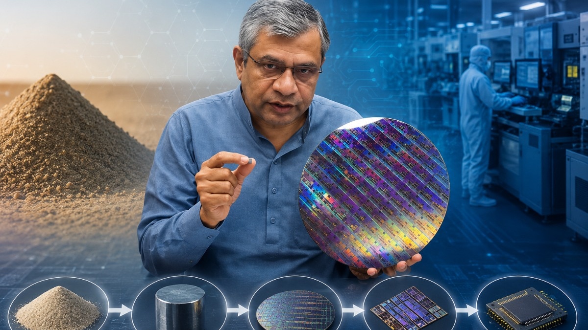
Vaishnaw Explains India’s Journey From Sand to Semiconductor Chips

India’s Semiconductor Push Advances With Tata’s Dholera Fab

India's Breakthrough: Indigenous Single-Crystal Jet Engine Blade Technology

Xiaomi Expands Chipmaking With Xring O3 and TSMC

SMIC Raises Chip Prices as AI Demand Boosts Record Revenue