

Science & Tech · Science & Environment · 2 hrs ago
South Korean team controls 2D crystal growth with over 99% success
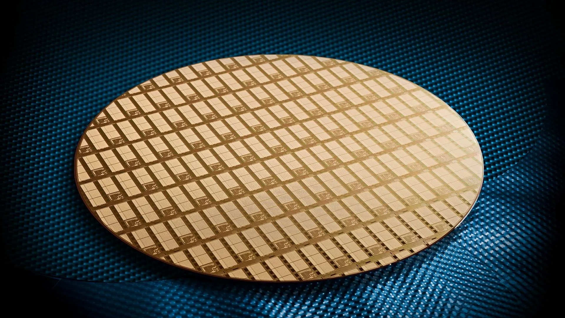
A team led by the Korea Advanced Institute of Science and Technology in South Korea developed a method to control where tiny semiconductor crystals begin growing.
The method placed individual crystals at chosen spots in over 99% of 400 patterns using molybdenum disulfide, a material only a few atomic layers thick.
Oxygen released from an oxide barrier suppresses unwanted growth, helping one crystal form at the center of each patterned area.
This could help prevent grain boundaries, where separate crystals meet and disrupt the movement of electrons.
The work matters because very thin semiconductor layers could one day be stacked to bring computing and memory components closer together.
The team has not built a stacked processor or shown faster, more energy-efficient computing, and the method still needs development before it can be used in large-scale manufacturing.
Further work must test whether the technique can fit into semiconductor production at scale.

Researchers in South Korea developed a method that controlled where individual molybdenum disulfide crystals formed with more than 99% success across 400 patterned regions.
The technique uses oxygen released from an oxide barrier to suppress unwanted crystal growth and favor formation at a central point.
The team said the method could help address challenges in making vertically stacked chips, which require precise semiconductor growth on existing circuits.
Researchers also demonstrated selective deposition of a thin ruthenium film on molybdenum diselenide regions.
The study did not demonstrate a complete stacked processor or measure changes in computing speed or energy use.
- Who
- A team led by the Korea Advanced Institute of Science and Technology, working with UNIST, Hanyang University and TDS Innovation.
- What
- The team developed a method to control where individual crystals form, with more than 99% success across 400 patterned regions.
- When
- The study was published October 8. The article was published October 13, 2026.
- Where
- South Korea.
- Why
- The method could help enable precise growth of semiconductor layers for vertically stacked chips.
This story does not have two clearly opposing sides.
The study was published in Nature.
Interesting Engineering published its article about the technique.
- Success rate
- More than 99% across 400 patterned growth regions
- Semiconductor material
- Molybdenum disulfide (MoS₂)
- Growth method
- Etching-flux-mediated single-centered nucleation (EF-SCN)
- Oxide barrier example
- Hafnium oxide (HfO₂)
- Selective metal deposition
- Ruthenium formed on molybdenum diselenide (MoSe₂) regions
Related
High-speed video shows how detached honeybee stingers keep pumping venom
2 hrs ago · 6 sources

Isle of Wight fossil identified as a new megaraptoran dinosaur
2 hrs ago · 3 sources

AI data centers face rising insurance risks as construction expands
53 mins ago · 2 sources

A sharper ear may help adults learn second-language sounds
2 hrs ago · 2 sources