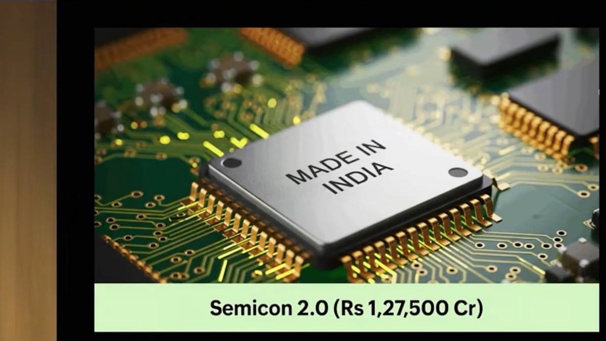

2 hrs ago
HCLTech Launches ₹185 Crore Advanced Semiconductor Lab in Bengaluru

HCLTech has opened a new laboratory in Bengaluru for working on computer chips.
The company is investing ₹185 crore in the facility.
The lab covers 40,000 square feet and contains specially clean rooms.
Engineers will test chips, check their quality and find problems.
The facility can support work from early research through production preparation.
It uses equipment from several technology companies.
HCLTech says this will help customers receive solutions faster.
The lab is also part of growing efforts to expand India’s semiconductor industry.

HCLTech announced a ₹185 crore investment in an advanced semiconductor lab in Bengaluru.
The 40,000-square-foot facility includes 25,000 square feet of Class 10K and Class 1K cleanrooms.
The lab will provide post-silicon engineering, advanced testing, electrical validation, qualification and failure analysis.
Equipment from Teradyne, Advantest, Keysight, Tektronix and Thermo Fisher Scientific supports research, pre-production and production qualification.
The facility is intended to accelerate semiconductor innovation and support India’s goal of becoming a global technology hub.
- Who
- HCLTech, or HCL Technologies, announced the facility.
- What
- The company launched an advanced semiconductor lab involving a ₹185 crore investment.
- Where
- The lab is located in Bengaluru, India.
- When
- The announcement was made on Tuesday and published on September 8, 2026.
- Why
- HCLTech said it aims to advance semiconductor innovation, accelerate time-to-market for global clients and strengthen India’s semiconductor capabilities.
Key facts
- Investment
- ₹185 crore
- Location
- Bengaluru, India
- Facility size
- 40,000 square feet
- Cleanroom space
- 25,000 square feet of Class 10K and Class 1K cleanrooms
- Core capabilities
- Post-silicon engineering, advanced testing, qualification and failure analysis
- Equipment providers
- Teradyne, Advantest, Keysight, Tektronix and Thermo Fisher Scientific
- Related government program
- ₹1.27 lakh crore Semicon 2.0 programme
Quotes
Hari Sadarahalli
Corporate Vice President and Global Head of Engineering and R&D Services at HCLTech
“With two decades of semiconductor expertise, HCLTech’s new 40,000 sq ft advanced semiconductor lab, featuring 25,000 sq ft of Class 10K and 1K cleanrooms, delivers end-to-end post-silicon engineering, advanced testing and failure analysis”
 thehindubusinessline.com
“This facility reflects our deep commitment to investing in high-end engineering capabilities. We are excited to contribute to the country’s vision of becoming a global hub for advanced technology”
thehindubusinessline.com
Sources
Related news
HCLTech Invests Rs 185 Crore in Advanced Semiconductor Lab Bengaluru

India’s Semicon 2.0 Broadens Chip Ecosystem; Three Stocks Watched
India Notifies Rs 1.27 Lakh Crore Semicon 2.0 Programme
India Expands Semicon 2.0 With 100,000 Engineer Target

India Notifies ₹1.27 Lakh-Crore Semicon 2.0 Semiconductor Expansion Scheme