

Archive · 26 Jul 2026
India Faces Tech and Capital Hurdles in 2 nm Chip Roadmap
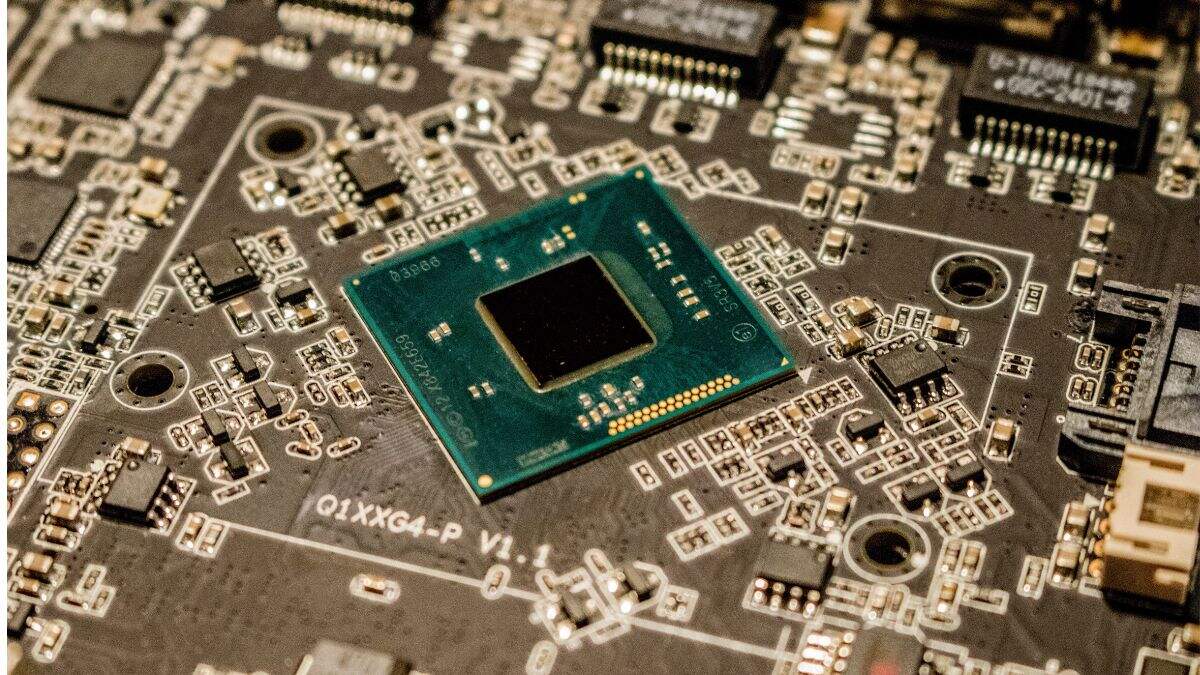
India wants to make smaller and more advanced computer chips, going from 28 nm to 2 nm.
But there are big challenges.
First, they need the right technology and a lot of money.
They also need skilled workers and special machines called lithography equipment.
Some people think India should focus on making older, simpler chips first to build a strong base.
Others think India should aim for the most advanced chips right away, like Japan is doing.
The government says they will focus on research and not just buy technology from other countries.
Right now, most computer chips used are older types, so India wants to be a leader in making those while also working towards making the newest chips.

India aims to advance from 28 nm to 2 nm chips but faces challenges in technology transfer, capital, talent, and access to advanced lithography equipment.
Tata Electronics' Dholera fab is currently building capacity in the 28 nm to 110 nm range.
India's government and industry executives debate whether to focus on advanced nodes immediately or strengthen the legacy node ecosystem first.
Global chip demand is 70% for legacy nodes, with China leading in this segment.
Costs roughly double at each node, making advanced chip production expensive.
- Who
- Indian semiconductor industry executives and government officials
- What
- Challenges in advancing from 28 nm to 2 nm chips
- When
- Current and future plans
- Where
- India
- Why
- To become a significant player in the global semiconductor industry
Advocates for Immediate Advanced Node Development
Proponents of Strengthening Legacy Node Ecosystem
Technology and Capital Investment
Advocates for Immediate Advanced Node Development
India should aim for advanced nodes like 2 nm directly, following Japan's Rapidus model, to stay competitive.
Proponents of Strengthening Legacy Node Ecosystem
India should focus on deepening the broader semiconductor ecosystem before racing to advanced nodes.
EUV Access and Technology Transfer
Advocates for Immediate Advanced Node Development
Government-to-government engagement is necessary to secure access to advanced lithography equipment.
Proponents of Strengthening Legacy Node Ecosystem
The priority should be on building a strong foundation in design, packaging, materials, equipment, and IP.
- Current Advanced Project
- Tata Electronics' Dholera fab (28 nm to 110 nm)
- Government Goal
- 7 nm and eventually 2 nm chips
- Critical Challenges
- Technology transfer, capital, talent, and access to advanced lithography equipment
- Global Advanced Node Operators
- Three companies worldwide, with Japan's Rapidus as the newest entrant
- Global Chip Demand
- 70% for legacy nodes, led by China
- Cost Doubling
- Costs roughly double at each node (28 nm to 14 nm, 7 nm, 3-4 nm)